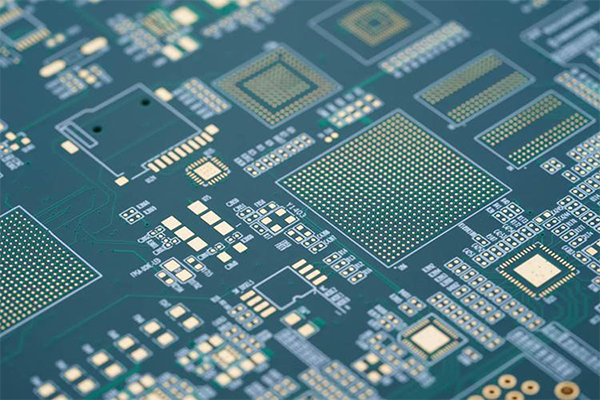
PCB's and products are not always clean when they arrive to the production floor. Surface contaminants such as oxides or other contaminatns may be present that can reduce the adhesion or wetting of fluids. Surface treatment technology can eliminate these contaminants.
Due to the rapid development of various electronic industries, production processes have increasing stringent technical requirements for the products being used. PCB surface treatment technology not only addresses organic contaminants and metal oxides on the surface of products but also performs surface activation treatment. This ensures adhesion between materials and resolves process pain points such as insufficient adhesive flow, unreliable conductivity, difficult coating, and inadequate soldering strength.
 Process characteristic
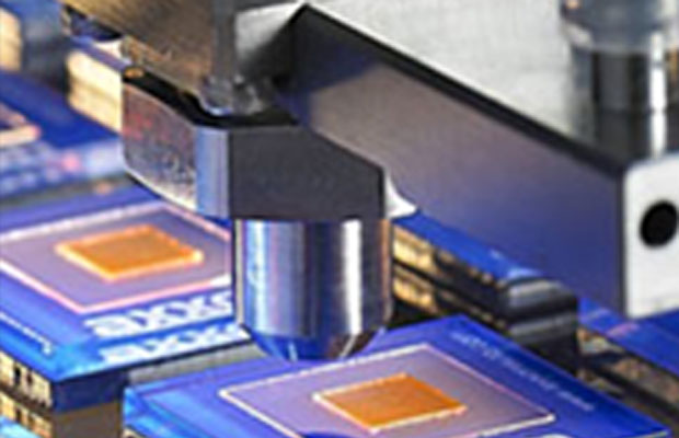
The application principle of atmospheric plasma surface treatment involves ionizing oxygen or hydrogen gas using radio frequency power to form oxygen ions and hydrogen ions. These ions chemically react with organic contaminants or metal oxides on the product surface forming gaseous carbon dioxide and water vapor that are then removed. Ultimately, this process achieves the goal of removing contaminants and activating the product surface.
Plasma surface treatment is typically used to remove organic contaminants from non-metallic product surfaces, remove metal surface oxides, and activate product surfaces. It demands high standards for plasma technology application.
Key points of plasma surface treatment technology include:
1. Various chemical processes effectively remove organic contaminants and metal oxides from product surfaces, activating the product surface (WCA<20° for LEDs/PCB substrates).
2. 100% safe and environmentally friendly, with no ion bombardment, low temperature, low pressure, no ESD, no arcing, no splashing, no water ripples, and no UV damage.
3. Batch processing in-line to ensure production efficiency, capable of processing in atmospheric environments and easy to maintain.
4. No dust particle contamination on product surfaces.
5. Will not cause damage or roughness changes to sensitive product surfaces.
6. Choose different platforms according to different product applications to ensure efficiency and flexibility.
7. Compatible with different product sizes for production and rapid switching to ensure compatibility.
Atmospheric plasma surface treatment technology is applied in industries such as semiconductor, automotive electronics, consumer electronics, and LEDs. Innovative plasma technology presents significant opportunities to replace traditional plasma technology. Equipment capacity and stability are crucial for production enterprises. Atmospheric plasma systems can be configured with different size heads for compatability with different product geometries. For the best solutions, combine Axxon Mycronic dispensing and Axxon Mycronic Atmospheric Plasma Treatment.
 You may also be interested in