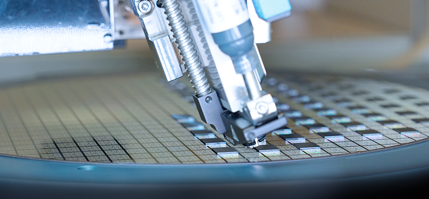
In the new era of ubiquitous connectivity, the functionality and performance of electronic products are becoming more robust, placing higher demands on core components such as computing power, storage capacity, processing power, and display capabilities. The quest for excellence is evident in every aspect. Integration must be compact, software functions must be powerful, performance must be stable and outstanding, and entertainment must be innovative. The comprehensive capability of the products is a challenge that tests the consumer's willingness to invest. The intervention of dispensing technology serves as the perfect coordination bridge for various components, ensuring the ultimate stability and reliability of products through bonding, thermal conduction, sealing, and more.
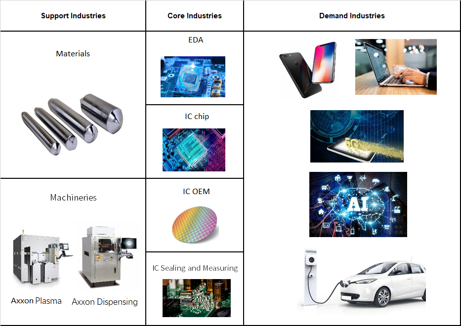
Common electronic products such as computers, smartphones, watches, tablets, etc. are all closely related to semiconductors. Semiconductor components are widely used in various fields, including computers, communications, and consumer electronics (3C). The development of the industry can be divided into three main parts: demand industry chain, core industry chain and support Industry Chain.
Demand Industry Chain: This is the fundamental driving force of the industry's development, which includes products such as smartphones, watches, PCs, automotive electronics, 5G technology, artificial intelligence (AI), and the Internet of Things (IoT).
Core Industry Chain: This includes the design and manufacture of semiconductor products, including processes such as wafer fabrication in the front-end and packaging and testing in the back-end.
Support Industry Chain: This includes materials, equipment, clean engineering, etc., which provides the necessary tools, raw materials, and production environments for the manufacture of IC (integrated circuit) products.

As a member of the support industry chain, Axxon's process solutions are widely used in various applications in the semiconductor industry, including
1.Wafer Fabrication Dispensing (Wafer Fab): This plays a critical role in the manufacturing process of semiconductor chips. It not only provides a secure bond and protection between the chip and the substrate, but also helps to improve the performance and reliability of the chip.
2. Wafer-Level Packaging (WLP): WLP effectively increases production efficiency and reduces costs by packaging multiple chips on a single wafer instead of individual packages. It also reduces the size and weight of semiconductor devices, increasing chip integration and performance. Axxon's solutions are widely used in various electronic devices such as smartphones, tablets, laptops, televisions and smart homes.
3. Flip Chip Ball Grid Array (FCBGA): This packaging format, also known as flip chip ball grid array, is a primary packaging format for graphics processing units (GPUs) and other semiconductor chips. The bottom of the chip is covered with solder balls. To ensure the stability of each ball's bond to the substrate, the main dispensing application is the underfill process. This process integrates the integrated circuit (IC) with the substrate, minimizing the effects of thermal expansion and contraction of the substrate.
4. Flip Chip Chip Scale Package (FCCSP):
Flip Chip is a semiconductor packaging technology in which the chip is flipped over and bonded to the packaging substrate by solder ball joints. In dispensing encapsulation, a layer of adhesive is applied between the flipped chip and the substrate to hold it in place.
The benefits of dispensing encapsulation include
- Improved reliability and performance of the chip: Dispensing helps provide shock resistance, moisture resistance, and thermal insulation, reducing the failure rate of the chip due to environmental changes.
- Increased chip density and interconnect count: Dispensing enables a tighter bond between the chip and the substrate, increasing the number of interconnection points between them.
- Reduced manufacturing costs: Dispensing encapsulation eliminates the need for interconnect devices such as wire bonds, reducing manufacturing costs.
However, dispensing encapsulation also has some drawbacks, such as the thickness of the dispensed material, which affects the chip's heat dissipation, and the need for greater manufacturing expertise and precision control of the dispensing process.
5. System in Package (SiP): By integrating multiple chip modules, SiP optimizes system performance, eliminates redundant packaging, shortens design cycles, reduces costs and increases integration. UV adhesive encapsulation is a key dispensing process that tightly seals multiple modules together to prevent water, dust and dislodgement.
6. Power Device IGBT Module Package: These are used in high-voltage, high-current motor drive applications such as high-speed trains, EMUs and new energy vehicles. Dispensing applications include potting and thermal conduction to ensure bubble-free potting and good contact and dissipation of heat components.
7. Leadframe Package: This is the base material for semiconductor packaging and serves as the chip carrier for integrated circuits. Dispensing applications include chip bonding, silver paste, solder paste and conductive adhesive.
8. Leadframe Package: Shell Case Packaging and other packaging methods, including processes such as Plasma for Wafer Hybrid Bonding, Flip Chip Underfill, Dam & Fill, Glob Top, Flux Spray, Solder Paste/Silver Paste Coating, EMI Shielding, TIM dispensing on chips, Potting, etc.